Physical Address
304 North Cardinal St.
Dorchester Center, MA 02124
Physical Address
304 North Cardinal St.
Dorchester Center, MA 02124

Discover the 10 best silicon wafers in 2026, from decorative display pieces to research-grade substrates and protective carriers. Our picks cover collectors, engineers, and students.
You want a real silicon wafer. Maybe it's to pin to your office wall as a conversation starter. Maybe you need a clean substrate for a thin-film deposition run. Or maybe you already have a wafer and need a proper box to keep it from gathering dust (or breaking). The problem is that the average Amazon search for "silicon wafer" throws back a baffling mix: decorative display pieces with microchip patterns, technical prime-grade substrates with detailed specs, and oddly specific carriers that only fit certain diameters.
Whether you are a collector looking for the best silicon wafers to display on your desk, a researcher needing a specific resistivity substrate, or a hobbyist who just wants to see what a real chip looks like, the range of options can be overwhelming. This roundup covers ten products that cover the full landscape: authentic integrated circuit wafers etched with copper patterns, polished intrinsic pieces for educational experiments, prime-grade wafers with tight tolerances for lab use, and dedicated storage carriers to protect whatever you buy.
TL;DR: The Esthepro 12 Inch is the most visually striking decorative wafer for display. The Alpha Nanotech 2 Inch (Qty 1) is the best entry point for lab and teaching use. The Ruiysion 12 Inch Wafer Box is the essential storage solution for protecting large wafers. The Innconee 12 Inch Double-Sided Polished Wafer offers a premium polished finish for collectors.
| # | Product | Key Spec | Best for |
|---|---|---|---|
| 1 | Esthepro 12 Inch | 12 inch, copper process, uncut IC wafer | Decorative display, large statement piece |
| 2 | Esthepro 8 Inch | 8 inch, copper process, uncut IC wafer | Smaller decorative display |
| 3 | Moderock 5 Inch | 5 inch, double-side polished, no circuit pattern | Minimalist desk art or teaching aid |
| 4 | Innconee 12 Inch | 12 inch, double-side polished, genuine IC wafer | Premium polished display, STEM education |
| 5 | XUSILAOK 10x10mm Intrinsic | 10x10mm, undoped high-resistivity silicon | Research, material science experiments |
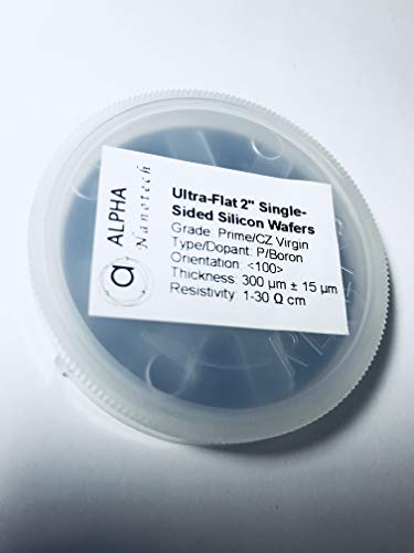
| 6 | Alpha Nanotech 2 Inch (Qty 1) | 2 inch, prime-grade, P/Boron, single-side polished | Lab use, single experiment, process development |
| 7 | Alpha Nanotech 2 Inch (Qty 10) | 2 inch, prime-grade, P/Boron, pack of 10 | Bulk lab use, teaching classes, repeatability |
| 8 | Alpha Nanotech 4 Inch Double-Side | 4 inch, double-side polished, N-type | MEMS, photonics, double-side processing |
| 9 | Ruiysion 12 Inch Wafer Box | 12 inch single-wafer carrier | Storing and protecting a large wafer |
| 10 | Ruiysion 1 Inch Carrier 10-Pack | 1 inch carriers, 10 pack with spring | Organizing multiple small wafers |

Pros
Cons
Best for: Collectors and tech enthusiasts who want a visible, conversation-piece wafer for desk or wall.
Check current price on Amazon →
The 12-inch Esthepro is the largest decorative wafer in this roundup, and it makes an immediate impression. The copper process creates an intricate, colorful microchip pattern that catches light and draws the eye. It's a genuine uncut integrated circuit wafer, not a replica, which adds authenticity for anyone who appreciates semiconductor history. The size is substantial enough to be the centerpiece of a tech-themed display. That said, the supplier notes that the exact pattern can vary from the product images, so what you get may differ slightly. And this is strictly a display piece — the listing explicitly states no guarantee for research applications. If you want a wafer to actually use in a lab, look to the Alpha Nanotech or XUSILAOK options.

Pros
Cons
Best for: Those who want the Esthepro look but have less space or want a more modest display piece.
Check current price on Amazon →
The 8-inch Esthepro shares the same copper-based microchip pattern as its larger sibling, but in a more manageable size. The core features are identical: a genuine uncut wafer made with 90–130 nm copper technology on a silicon substrate. For a desk or shelf where 12 inches feels too dominating, this is a more proportionate fit. The trade-off is obvious — the smaller surface area means less of that mesmerizing, reflective pattern. But for a gift or personal collection piece, it still delivers the wow factor. Like the 12-inch version, pattern consistency isn't guaranteed, and it's not intended for any functional use.

Pros
Cons
Best for: Anyone who wants a clean, polished wafer to use as a teaching aid or minimalist desk art.
Check current price on Amazon →
The Moderock wafer is a straightforward, no-frills silicon disc. Its standout feature is the double-side polish, which gives both surfaces a smooth, reflective quality. That makes it more versatile for display — you can flip it, mount it in a frame, or use it in an optical demonstration. At 5 inches, it's small enough to fit in a shadow box or on a narrow shelf. The lack of features listed on the product page suggests it's a simple polished wafer without an integrated circuit pattern, so it won't have the intricate microchip aesthetics of the Esthepro wafers. It's more of a raw silicon canvas, which could appeal to purists or educators who want to show the base material before circuits are fabricated.

Pros
Cons
Best for: Collectors and STEM educators who want a large, high-quality polished wafer to admire or teach with.
Check current price on Amazon →
The Innconee 12-inch wafer goes a step beyond most decorative options by emphasizing the double-side polishing and the light interference patterns that result. It's described as a genuine uncut IC silicon wafer, so it's the real deal. But unlike the Esthepro wafers, which have a visible copper circuit pattern, the Innconee seems to focus more on the polished substrate itself, with rainbow-like reflections under different lighting. That makes it a more subtle, elegant display piece — less "look at this chip" and more "look at this material." The included note about fragility is worth heeding; at 12 inches and only a fraction of a millimeter thick, these wafers can crack easily. For a classroom or lab where you want to demonstrate wafer properties, this is a solid pick.

Pros
Cons
Best for: Researchers, students, and hobbyists who need a small, undoped silicon substrate for material studies or electrical characterization.
Check current price on Amazon →
This is a fundamentally different kind of product from the decorative wafers above. The XUSILAOK listing sells intrinsic (undoped) silicon substrates designed specifically for research use. The particular variant here is a 10x10mm square piece cut from a larger wafer, with high resistivity and no dopant additives. That's essential for certain electrical measurements and material science experiments where you need a pure baseline. The product is available in larger diameters (1 to 8 inches) if you order a different option, but this entry-level piece gives you a usable sample. It's not a polished display piece — the image shows a small, off-white square. But for a university lab, a makerspace, or any setting where you need to characterize intrinsic silicon, it's exactly the right tool.
Pros
Cons
Best for: Lab technicians, students, and researchers who need a high-quality, specification-guaranteed 2-inch wafer for one-off experiments or process development.
Check current price on Amazon →
Alpha Nanotech supplies prime-grade wafers with detailed specifications: P/Boron doped, orientation 100, thickness 300 um, with front surface polished and back surface etched. The total indicator runout (TIR) is under 3 um, total thickness variation under 10 um, and surface roughness under 0.5 nm. These are the numbers that matter to anyone working in a cleanroom or semiconductor lab. This single-wafer option is ideal when you only need one substrate for a small run or a proof-of-concept. The single-side polish is standard for many applications — you get a mirror finish on the active side and an etched backside. If you need double-side polish, you'll want to look at the 4-inch Alpha Nanotech wafer instead.

Pros
Cons
Best for: Laboratories, universities, or hobbyists who need multiple identical wafers for repeatability or class sets.
Check current price on Amazon →
This is essentially the same 2-inch prime-grade wafer as the single, but in a pack of 10. The specifications are identical: P/Boron, orientation 100, front polished, back etched, with tight tolerances. The advantage here is consistency — if you're running a series of experiments where wafer-to-wafer variation must be minimized, ordering a batch from the same supplier helps. It's also practical for teaching labs where a dozen students each need their own substrate. The downside is the upfront quantity — if you only need one or two, the single pack is more sensible. And you'll want to invest in a proper wafer carrier to store the unused ones, like the Ruiysion carriers also on this list.

Pros
Cons
Best for: Researchers who need a double-side polished wafer for processes that require both surfaces to be smooth, such as MEMS or optical applications.
Check current price on Amazon →
This 4-inch wafer from Alpha Nanotech is double-side polished, which sets it apart from their 2-inch offerings. Double-side polish is important for applications where you need to process or bond both sides of the substrate — common in MEMS, photonics, and some device fabrication. The wafer is N-type with phosphorous dopant, orientation 100, and comes with the same tight tolerances as the 2-inch wafers. The 4-inch size is a good middle ground: large enough for multiple die or more complex experiments, but not so large that it requires special handling equipment. Note that Amazon categorizes this under "Wafer Cookies," which is obviously a data error, but the product itself is a genuine semiconductor substrate. If you're a researcher looking for a double-side polished wafer at a moderate size, this is one of the few readily available options.

Pros
Cons
Best for: Anyone who owns a 12-inch decorative or lab wafer and needs a safe, clean place to store it when not on display.
Check current price on Amazon →
If you've bought a 12-inch wafer — decorative or research-grade — you quickly realize how fragile and exposed it is. The Ruiysion 12-inch single-wafer carrier solves that. The box is made from transparent plastic, so you can see the wafer without opening it. The interior has raised edges that keep the wafer centered and a secure locking lid that prevents accidental opening. It's compact enough to fit on a shelf or in a drawer. The main limitation is that it only holds one wafer. If you have multiple 12-inch wafers, you'll need multiple boxes. But for protecting that one prized display piece or a critical lab substrate, it does the job well.

Pros
Cons
Best for: Researchers or collectors who work with 1-inch wafers and need multiple storage units for organization and transport.
Check current price on Amazon →
The Ruiysion 1-inch carriers are designed for the smallest standard wafer diameter. Each carrier comes as a three-piece set: container, cover, and a spring that holds the wafer in place. The material is polypropylene with a claimed 100-class cleanliness, suitable for storing clean substrates. The 10-pack is practical for labs that handle many small wafers, or for educators who want to distribute samples to students. One thing to note: the spring mechanism can apply uneven pressure if the wafer isn't centered perfectly, so careful placement is required. And 1-inch wafers are less common than 2-inch or larger diameters, so make sure your wafers actually match this size before purchasing.
Buying a silicon wafer is more complicated than picking the first listing that matches your desired diameter. The right choice depends entirely on what you intend to do with it. Here are the key factors to weigh.
The single most important question is whether you need a wafer for display, for research, or as an accessory for storage. Decorative wafers like the Esthepro and Innconee products are genuine IC wafers, but they are sold specifically as collectibles or teaching tools. They have no guarantee of performance for any functional application. Research-grade wafers from Alpha Nanotech and XUSILAOK come with detailed specifications for resistivity, doping, orientation, and surface finish. They are intended for deposition, etching, characterization, and other lab processes. Wafer carriers are a separate category altogether — they protect your investment and prevent contamination. Mixing these categories up can lead to frustration: buying a decorative wafer expecting it to work in a cleanroom will disappoint, and buying a research wafer just to pin it on the wall is overkill.
Wafer size affects everything from visual presence to experimental compatibility. For display purposes, larger diameters like 12 inches create a more impressive piece, but they are also more fragile and harder to store. The 8-inch and 5-inch options are more practical for desk displays. For research, standard diameters are 2 inches, 3 inches, 4 inches, and 6 inches, with 2 inches being the most common entry-level size for university labs and hobbyists. A 2-inch wafer fits in many spin coaters, evaporators, and other process tools. The 10x10mm intrinsic piece is useful for quick tests but too small for most fabrication steps.
The surface finish determines what you can do with the wafer. A polished front surface gives a mirror-like smoothness needed for photolithography and thin-film deposition. An etched back surface (rougher) is typical for single-side polished wafers. Double-side polished wafers have both surfaces smooth, which is required for applications where you need to process or bond both sides, such as MEMS devices, optical windows, or transmission measurements. If you just want to look at a wafer, double-side polish adds aesthetic appeal but isn't necessary. If you want to actually fabricate something, check which side needs to be polished and whether the backside roughness matters for your process.
For research use, the type and concentration of dopant (or lack thereof) is critical. Intrinsic (undoped) wafers have high resistivity and are used as a baseline for electrical measurements, radiation detectors, or when you need minimal free carriers. Doped wafers are categorized as N-type (phosphorous, antimony, arsenic) or P-type (boron). The resistivity range (e.g., 1–30 ohm·cm) determines carrier concentration. The Alpha Nanotech wafers on this list are P-type (boron) with a specified resistivity, while the 4-inch double-side polished wafer is N-type (phosphorous). Make sure the doping matches your experiment's requirements, or choose an intrinsic wafer if you need to control that variable yourself.
Even decorative wafers are fragile. Silicon is brittle, and a thin 300 um wafer can crack if dropped or bumped. Proper storage in a wafer carrier prevents scratches, contamination, and breakage. Carriers come in different sizes and materials: single-wafer boxes for large diameters, and multi-wafer shippers for smaller sizes. The Ruiysion carriers are made of polypropylene and claim 100-class cleanliness, which is adequate for most storage needs. If you plan to transport wafers, look for carriers with springs or foam that hold the wafer securely. Never stack wafers directly on top of each other — use individual carriers or separators.
Silicon wafers are the fundamental substrate for manufacturing integrated circuits and most semiconductor devices. They serve as the base upon which microelectronic circuits are built through processes like doping, etching, and deposition. Outside of fabrication, wafers are also used as substrates for MEMS, photonics, solar cells, and as educational tools or decorative pieces.
Not reliably. Decorative wafers like the Esthepro and Innconee are sold as display objects, not as functional substrates. They may have unspecified resistivity, surface quality, or contamination levels. For any experiment requiring known electrical properties or cleanliness, stick with prime-grade wafers from suppliers like Alpha Nanotech or XUSILAOK that provide detailed specifications.
Store wafers in a dedicated wafer carrier or box with a secure lid. The carrier should hold the wafer by its edges to avoid touching the surfaces. Keep it in a clean, dry environment away from dust and moisture. For long-term storage, a container with a spring or foam cushion is recommended to prevent movement and breakage.
A polished surface has been mechanically and chemically smoothed to a mirror finish. This is the side where lithography and processing occur. An etched surface is rougher, created by chemical etching to remove damage from slicing. Most prime-grade wafers are polished on the front and etched on the back. Double-side polished wafers have both sides polished for applications requiring optical transparency or bonding.
All the wafers in this roundup are genuine silicon wafers, not plastic replicas or models. The Esthepro and Innconee wafers are actual uncut integrated circuit wafers from semiconductor fabrication. The Alpha Nanotech and XUSILAOK wafers are prime-grade or intrinsic substrates used in research and industry.
Prime-grade refers to the highest quality classification for virgin silicon wafers. These wafers come directly from a single crystal silicon ingot, have tightly controlled specifications for thickness, flatness, and surface roughness, and are free from defects like scratches or particles. Prime-grade wafers are suitable for critical semiconductor processing where consistency matters.
Yes. Standard packaging or envelopes do not protect wafers from physical damage or contamination. A wafer carrier designed for the correct diameter prevents edge chipping, surface scratches, and exposure to particles. For lab use, ESD-safe or cleanroom-compatible carriers are even better. For home display, a simple plastic carrier like the Ruiysion boxes provides adequate protection.
Choosing the best silicon wafer comes down to your goal. For a striking decorative piece that shows the beauty of semiconductor manufacturing, the Esthepro 12 Inch is the most dramatic option, with its intricate copper pattern and large size. If you need a substrate for actual research or teaching, the Alpha Nanotech 2 Inch (Qty 1) gives you prime-grade specifications and tight tolerances at a very practical size. For storing and protecting a wafer you already own, the Ruiysion 12 Inch Wafer Box is the essential accessory.
If you're still unsure, start with a single 2-inch prime-grade wafer from Alpha Nanotech — it's the most versatile choice for anyone who wants to get their hands on a real, spec-guaranteed substrate. From there, you can branch out into decorative wafers for display or invest in carriers as your collection grows. The world of silicon wafers is surprisingly deep, and this roundup covers the key entry points for both curiosity and serious work.
This article contains Amazon affiliate links. We may earn a small commission on qualifying purchases at no extra cost to you.